![]()
|
Welcome to the Shivaram Group Research Pages |
|
|
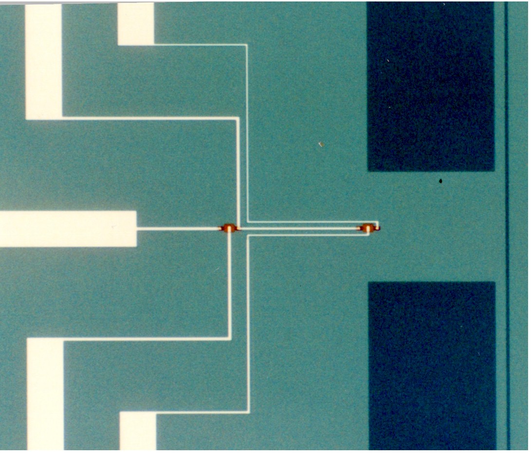
Research and development of MEMS (micromechanical sensors) has mushroomed into gigantic proportions in recent years. While progress in this field is driven by commercial concerns of equal importance is the use of MEMS in basic materials research. MEMS devices in existence today may be considered as a particular example of a more general class of lab-on-a-chip devices. An example of a MEMS devices we have fabricated is shown in the figure below. It is a simple cantilever which extends from the base of the wafer on the middle right side of the picture. Two FETs have been designed into the silicon wafer (these are seen as reddish brown dots in teh figure) one at the base of the cantilever (right FET) and the other on the wafer (left FET). Motion of the canilever (into and out of the page) causes a differential voltage to appear across the FETs. The origin of this differential signal is the strain dependence of the FET characteristics. Thus compared to the passive piezocantilevers available in the market today these devices have a integral built in amplifier on them.
Photomicrograph of a 100 micron x 100 micron integrated silicon AFM cantilever, Chaparala, Jones and Shivaram. |
|
Send
mail to bss2d@virginia.edu with questions or comments about this web site. |