INTRODUCTION: BOOLEAN ALGEBRA AND DE MORGAN'S LAW
There are certain statements that can only be either true or false. Example: The statement today is Friday" is either true, (when made on a Friday), or false, (when made on any other day of the week). A British mathematician, George Boole (1815-1864) created the field that is today known as "Boolean Algebra" by showing that statements such as the one above can be manipulated in a formal, algebraic, manner. While Boolean Algebra has nothing directly to do with physics it is the basis of a field often referred to as electronic logic that has widespread applications in electronic engineering, computer design and experimental nuclear and particle physics. This makes it worthwhile for us to discuss it briefly in the context of some experiments about digital electronics.
Returning to the statement today is Friday, we represent it symbolically with a logical variable A that has the value A = 1 when the statement is true or the value A = 0 when it is false. Now let us consider another statement: today is the 13th. This statement we represent with the variable B which has the value 1 on the 13th of each month and the value zero on any other day.
Next let us consider the conjunctions OR and AND. If we connect two logical statements with an AND that means that both are true. Thus, if you are superstitious you might say: if today is Friday the 13th (A = 1 AND B = 1) I will not travel. If you are very superstitious you might even say: if today is either a Friday or the 13th (A = 1 OR B = 1) I will not travel. In Boolean algebra one formally manipulates statements such as the ones above by representing the OR with an addition and the AND with a multiplication. Let Q be the result of such an algebraic manipulation. Then, on any Friday the 13th the statement.
Q = A × B = 1 × 1 = 1 ------------------------Eq. (1)
is true and if you are superstitious you might resolve that if
Q = 1 you will not travel. If you are very superstitious you might
even decide not to travel if
A + B $ 1 -----------------Eq. (2)
|
| |||
No statement can be truer than true. There is, therefore, no reason
that a logical variable should ever have a value greater than
unity and the paradoxical looking statement
1 + 1 = 1 ----------------------Eq. (3)
holds true in Boolean Algebra. All the above can be summed up
in the form of the Truth Table, Table 1.
The logical complement of the statement today is Friday
is the statement today is not Friday. If A represents the
original statement then its complement is customarily represented
by , pronounced 'A bar'. Obviously, if A has the value 1, has
the value 0 and vice versa. Based on this notation one can easily
verify de Morgan's laws, (A. de Morgan 1806 1871):
Convince yourself that these laws hold by studying Table 2.
Table 2: Truth table for de Morgan's Laws
| A'+B' | |||||||
All of this would, at best, be of interest to some logicians, were it not for the fact that there are circuit elements that one can identify with the statements and operators of Boolean algebra. This means that one can apply Boolean algebra to the design of logic circuits such as the ones that are used in computers. A simple toggle switch has only two states, open or closed, as shown in Fig.1.

Figure 1: a) open switch = 0 b) Closed switch =1
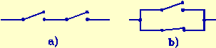
If one represents a logic 1 with a closed switch and a logic 0 with an open switch one can build circuits that represent logical operations. Fig. 2a shows an AND circuit in which a current flows only if the first AND the second switch are closed. Fig. 2b shows an OR circuit through which a current will flow if one switch OR the other is closed.
Figure 2: a) AND circuit. b) OR circuit.
In computers, electronic circuits take the places of mechanical toggle switches and AND and OR circuits, often called AND gates and OR gates, are represented by the circuit symbols shown in Fig. 3.
Figure 3: a) Symbol of an AND gate. B) Symbol of an OR gate.
Table 3: Truth table for exclusive OR
In circuit elements such as these a logic 1 is usually represented by one voltage level and a logic 0 by another. The conventions vary, but in a typical example (e.g. Transistor Transistor Logic, or TTL) a voltage level of V $ 2.4 V represents a "1" and V # 0.8 V represents a "0". In a TTL AND gate, Fig. 3a, the voltage at the output lead C will thus be 0 unless there is an input voltage of $ 2.4V applied to both input A AND input B, in which case it will go to 2.4 V. In an OR gate, such as shown in Fig. 3b, an input level of $ 2.4 V at either input A or input B (or both) will produce an output level of 2.4 V at the output C. If one employs switches that do not switch from off to on but that toggle between two different current paths, as shown in Fig. 4a, one can build a circuit that switches from one state to the other whenever either of the switches is actuated; see Fig. 4b. You can readily see that a circuit like this allows one to turn a light on and off from two ends of a hallway. In electronics this kind of circuit is known as an Exclusive OR, its circuit symbol and truth table are, respectively, shown in Fig. 5 and Table 3.
In electronic circuitry it is often convenient to have circuit
elements that invert the levels and thus give the logic
complements of the output signals. Fig. 6a shows the circuit symbol
for a NAND gate, (Not AND), a circuit that
represents the operation i.e. that produces an output level only
when there is no signal present at either input A or input
B. Fig. 6b shows a NOR gate representing the operation,
see Table 2.
APPLICATIONS
With the basic logic elements that we have introduced above
one can build a large variety of logic circuits, many of them
very ingenious (and quite complicated). In this lab we can only
give you a glimpse of the many possible applications that exist.
By far the most important application of digital electronic circuitry
is in the design of computers. We have already seen how logical
decisions based on the presence of individual (OR) or simultaneous
(AND) signals can be implemented. Other important capabilities
of a computer are the ability to remember things that it has been
told, and, of course, the ability to calculate, i.e. to add. (Subtraction
is simply an addition with the opposite sign, whereas multiplication
and division can be reduced to repeated additions and subtractions.)
THE FLIPFLOP
Consider a circuit consisting of two NAND gates, as shown
in Fig. 7. Let there be a positive input signal, a logic 1, present
at both terminals S and R. What will be the voltage level of the
output terminals Q and ? (Assuming that we are using TTL elements.)
Could both outputs be at the zero level? Let us investigate. The
outputs are connected crosswise to the second inputs, SN
and RN, of the two NAND gates. With
S and SN at the levels 1 and 0 respectively,
Q must be at the level 1, in contradiction with our assumption.
Could both outputs be at the level 1? With at the level 1, SN
must be 1 and Q = 0 which, again, contradicts the assumption.
Q = 0 and = 1 leads to SN
= 1, RN = 0, which would indeed lead
to Q = 0 and = 1, but how can that be? The circuit
and its inputs S and R are symmetrical, yet the outputs are not.
If Q = 0, = 1 is possible so must be the converse: Q = 1,
= 0. We have thus a bi-stable circuit, i.e.
one that can exist in two mutually exclusive but stable states.
Which of these two states the circuit occupies must depend on
its prior history. We investigate further. If we change the
level of S from 1 to 0 Q will flip to 1 which, in turn,
will force to flop to 0. Changing the input level of S
will thus cause the circuit to change from one of the two stable
states to the other. Restoring S to its original state 1 will
not make any difference, the circuit will remain in the second
state. The circuit can thus be permanently switched, or Set
by the application of a short pulse to the input S. Once
S has been restored to the 1 state further pulses to the S input
will have no effect. We can, however Reset the circuit
by the application of a short pulse to the R input. A flipflop,
such as this, can be used as a memory device: It will remember
the first pulse applied to the S input and it can be made to forget
by the application of a pulse to the R input.
A more mundane but important application of the simple flipflop
is the following: In a mechanical switch two metal contacts are
brought together when the switch is closed; it is almost unavoidable
that these contacts will bounce several times before they come
to rest upon each other. Each bounce will cause a short pulse
to enter the circuit. If the switch is used to turn on a light
that will not matter. If the switch is used in a computer keyboard
and enters "33333333" instead of "3" that
is intolerable. We have seen above that once a flipflop
has been flipped, further pulses will have no effect. It is, therefore,
a common practice in the design of electronic devices to follow
a mechanical switch with a flipflop that will debounce
it.
COMPUTING
We have already mentioned that subtraction, multiplication,
and division can all be reduced to addition. It will, therefore,
be sufficient for us to discuss the latter operation. The decimal
system, in which we normally carry out calculations, is not very
well suited to the use in computers. The fact that computers use
elements that are capable of only two states that we can identify
with zero and one suggests that we employ the binary
system.
In the binary system only the numerals 0 and 1 exist. Note:
these zeros and ones are numerals, not logical
variables. The rules of ordinary, not Boolean, algebra apply.
In case you have forgotten, Table 4 gives the first 10 integer
numbers in the decimal and the binary system.
| A | B | S | C |
| 0 | 0 | 0 | 0 |
| 0 | 1 | 0 | |
| 1 | 0 | 1 | 0 |
| 1 | 1 | 0 | 1 |
The rules of addition for binary numbers look strange due to the
fact that one has to carry an overflow whenever a digit
is larger than 1 e.g.:
1 + 1 = 10; 10 + 10 = 100; 11 + 11 = 110;
101 + 111 = 1100; etc.
Next we construct a circuit that will allow us to add binary numbers. Consider the parallel connection of an AND gate and an exclusive OR gate as shown in Fig. 8.
This circuit is known as a Half adder for reasons that will soon become clear.
We already know the truth tables for the individual elements and
we combine them in Table 5.
Next consider Fig. 9 in which several half adders are combined.
Imagine that the three digit binary numbers 110 were presented
to the inputs A0, A1, and A2,
(i.e. a 1 at A2, and A1, and a 0 at A0).
Now go back to Fig. 8 and assume that it represents the rightmost
half adder in Fig. 9. According to the truth table, Table 4, the
circuit is symmetrical in its response to input signals. That
means that even though it contains two different circuit elements
it does not matter which of the inputs A or B we identify with
A0 or B0. The outputs, however, behave differently
and we must identify S0 with the S(um) output. With
the number 110 present at the A inputs a 0 would be present at
input A0. If a 0 were also present at B0
both S0 and the carry output (which goes into the lower
half adder) would remain at zero. Entering a 1 at B0
would produce a 1 at S0 but would leave the carry output
at zero. In other words the last stage of this adding circuit
gives the correct answers to the problems 1 + 0, 0 + 1, and 0
+ 0. Had there been a 1 present at the A0 input, a
zero at B0 would have produced a 1 at S0,
whereas a 1 at B0 would have produced a zero at S0
and a 1 in the carry output which would have been fed into
the next half adder. This, of course, is exactly what the binary
addition 1 + 1 = 10 requires: a zero in the last place and a 1
that is carried to the next place. As an exercise investigate
how the circuit shown in Fig. 9 will respond if 111 is presented
to the A inputs and 110 to the B inputs.
BEFORE YOU START
You will assemble your circuits on the "OpAmp Designer"
breadboard, shown in Fig. 10, which has a fixed 5 V power supply
that you can use to power the integrated circuits. If you need
any help, please ask your instructor.
PLEASE NOTE: TURN THE 5 V POWER SUPPLY OFF BEFORE YOU PLUG
IN OR UNPLUG ANY I.C's. BEFORE YOU TURN ON THE POWER CHECK YOUR
CIRCUITS CAREFULLY. WHEN YOU ARE FINISHED WITH ONE EXPERIMENT
TURN THE POWER OFF BEFORE YOU CHANGE OVER TO THE NEXT.(A common
mistake is to connect power backwards. This will cause the I.C.
to get hot. If this happens, turn off the power, check the connection
and test the I.C. before proceeding.)
Figure 10
The small circles represent sockets. The lines show which of the
sockets are interconnected under the board. Features that are
not used in this experiment are crossed out. The integrated circuits
should be powered from the 5 V power supply on the left side of
the board.
Logic Levels. The following statements apply to the signal
levels at the input as well as the output pins:
! FALSE, or logic 0, is represented by a low potential (00.8 volts above the ground). Connecting an input terminal to ground puts it in the zero state.
! TRUE, or logic 1, is represented by a voltage of + 2.4 volts or more with respect to ground. Connecting an input terminal to such a potential puts it in the 1 state. An input can be set to the 1 state by connecting it to +5v through a 1000 W resistor, (do not connect directly to +5V!!!). If an input is left unconnected ("floating"), it will usually assume the logic 1 state. However, it is safer to force the input by applying a positive voltage or by connecting it to an output that is in the 1 state. This will avoid spurious signals by electrical noise.
! FANOUT. As many as 10 inputs may be tied to one output.
! NEVER connect two or more outputs together; the results are unpredictable and the I.C.'s can burn out. Connect outputs only to I.C. inputs.
! TIMING. Typical TTL
gates switch from one state to the other in 15 nanosec (1 nanosec
= 10-9 sec). This is the secret of a computer's high
speed.
The integrated circuits, chips or I.C's for short, that you will use are all of the TTL type. They usually contain four identical basic circuit elements. The pin assignments are shown in Fig. 11. This time the top view is given. The I.C's should be plugged into the two middle rows of sockets, straddling the center gap, so that each I.C. pin is connected to the four other sockets in its column. The two top and the two bottom rows should be connected to the 5 V power supply; both top rows to the two + 5 V connectors and both bottom rows to the ground connectors.
The input signals should be applied to the I.C's by connecting
their input pins by means of the two slide switches in the lower
right hand corner of the board to either 5 V (through a 1000 W
resistor) or to ground. To find out how the I.C's respond to these
input signals you must be able to read out the output signals.
This could be done by measuring the output levels with a voltmeter.
Instead you should use the Light Emitting Diodes or LED's
provided for this purpose. Since not all I.C's provide enough
power to light up the LED's you should first set up a Driver
circuit, using a 7406 I.C. as shown in Fig. 12.
WHAT TO DO
1). LED Driver. Plug a 7406 chip straddling the middle row near the right end of the board. Connect one LED through a 330 Ohm resistor to 5 V on one side and to one of the even numbered pins (other than 14) on the other, as shown in Fig. 12. Build a second, identical, circuit with one of the other 5 drivers. To test your two circuits connect the corresponding odd numbered pins through a 1 kW resistor to either + 5 V or ground. For the pin assignments see Fig. 11. Leave both circuits on the board, they will be used in the following experiments as indicators.
2). AND gate. Select a 7408 I.C and check its pin connections
in Fig. 11. Insert it in the board and connect pin 7 to ground
and pin 14 to +5V. Connect the center contacts of the two switches
to the two inputs of the gate and their upper contacts through
1 kW resistors to +5 V. Connect the
lower contacts of the switches to ground. Connect the output to
the LED driver. AFTER ALL CONNECTIONS HAVE BEEN MADE AND
CHECKED TURN ON THE POWER. Test the truth table for this
gate. Turn off the power.
3). OR, NAND, and NOR gates. Replace the 7408 I.C. successively
with a 7432, a 7400 and a 7402 I.C. (Note that the 7402 NOR gates
are reversed compared to the 3 other I.C's). Test each of these
gates and record their truth tables together with their wiring
diagrams in your notebook. Always give the I.C. pin numbers on
your wiring diagram as shown in Fig. 8. Any point in the circuit
diagram can then be found immediately on the breadboard. Troubleshooting
a complicated circuit is almost impossible without proper labeling.
(Don't forget to turn off the power before you switch I.Cs.)
4). FlipFlop. Construct the flipflop shown
in Fig. 7 from two of the NAND gates in a 7400 I.C. Connect one
LED driver each to the Q and Q Test it and see if it behaves as
described above.
5). Exclusive OR and Half Adder. Test one of the exclusive
OR gates on a 7486 I.C. and then connect it with one of the AND
gates in a 7408 I.C. to form the half adder shown in Fig. 8. Record
its wiring diagram and truth table in your notebook.