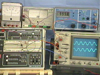
Build an a.c. voltage amplifier with a voltage gain of 10. A gain of 10 means that the ratio RC/RE should be equal to 10, as it was in the previous experiment. When no a.c. input voltage is applied, the transistor voltages and currents should be near the center of the operating range that you have determined earlier. Reasonable values would be VC ~ 5 volts, and IC ~ 10 mA, allowing for both a positive and a negative swing of the timevarying output signal. Given a supply voltage of 15 V, a collector voltage of VC = 7.5 V at a current of IC = 10 mA implies a 5 V drop across RC. RC should, therefore, be about 500 W. From RC = 500 W, follows RE = 50 W. The resistors used in the previous experiment, 470 and 47 W, are close enough. Using these values build the circuit of Fig. 11. The 47 W resistor is yellowpurpleblack and the 470 W resistor is yellowpurplebrown. Try to be neat to avoid wiring errors and accidental short circuits between adjacent wires. After you have turned down both power supplies connect them to your circuit. Check the circuit carefully - the layout of your circuit should look something like this - then turn on the power. Set the collector supply to 15 V, then raise the bias voltage until the bias current is ~ 50 mA. (With the 47 W and the 470 W resistor in series with the transistor it is safe to exceed 10 V on the collector supply.)
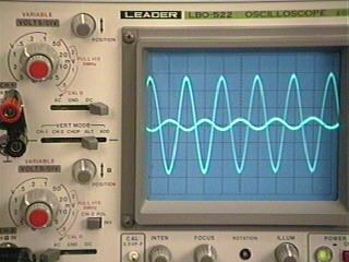
When the d.c. voltages and currents have been set you are ready to apply an a.c. signal: Connect one channel of the oscilloscope to the output of the oscillator and set the oscillator output to an amplitude of ~ 0.2 V. Be sure the dc offset control on the oscillator is set to zero. After verifying this value on the scope, connect the oscillator to the amplifier input. Connect the other channel of the oscilloscope to the Output terminal, i.e. to the collector, so that you can simultaneously view both the input and the output waveforms, using the ALT mode of the scope. As you probably know, a d.c. current cannot flow through a capacitor, but an a.c. current can. By using the 0.1 mF capacitor, as shown in Fig. 11, you can introduce an a.c. signal without altering any of the d.c. levels. The amplitude of the output voltage should be 10 times larger than that of the input voltage but cannot be exceed about 6 volts for any input amplitude. Why?
Once you have both the input and the output waveforms on the screen, compare their amplitudes using the calibrated sensitivity setting of the scope. (Be sure the variable sensitivity knobs on the scope inputs are in the fully clockwise CAL position.)
Now take another look at Fig. 10. As IB gets bigger, so does IC. However, a larger value of IC means a smaller value of VCE due to voltage drop across the series resistors, (47 W and 470 W). Indeed, IC cannot possibly get bigger than ICMAX = 15 V/(RC+RE) = 29 ma. Mark this value on your graph. Conversely, a small value of IB implies a small value of IC. A smaller IC in turn means a large value for VCE. The obvious limit is (VCE)max = 15 V, the voltage of the collector power supply. The intermediate values of IC and VEC one finds to lie along a straight line between the extremes. This straight line is the load line, shown in Fig. 10, and you should draw it on your graph.
The supply voltage V must equal the sum of the voltage VCE
across the transistor and the voltage drop across the two resistors
RC and RE.
V = VCE(IC) + IC(RC
+ RB)
We cannot readily solve that equation because we have only the
measured curves for the characteristic VC(IC),
not a mathematical expression. If we write the same equation in
the form
V - IC(RC + RB) = VCE(IC)
we have on the left the mathematical expression for the load line
as a function of the collector current, and on the right the expression
for the measured collector voltage as a function of the collector
current. The equal sign means that both expressions must be true
simultaneously, even if the second one is not known to us in a
mathematical form. We conclude that for any given base current
the collector current must be given by the intersection of the
characteristic for that base current and the load line. In other
words the load line lets us solve graphically the equation
that we could not solve mathematically.
Following are some suggestions for further exploration. Be systematic
and keep careful notes of your observations and measurements.
Take enough time to do a good job and don't feel that you have
to do everything. Be sure to leave the right power supply set
at 15 V.