1. Identify the emitter lead and plug it into the top row of one of the columns in the lower half of the board as shown in Fig. 9.

Figure 9:Layout of Transistor and leads on breadboard
2). Using the circuit shown below (which when layed out actually looks like this ) , map the characteristics of the transistor by injecting a known current into the base of the transistor.
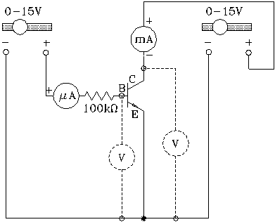
Figure 9:Circuit for Transistor Characteristics
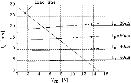
Figure 10: Transistor characteristics curve
b = IC/IB ------------Eqn.(3)
(Taking into account that you measured IC in milliamps
and IB in microamps, b should
be between 50 and 200.) Extract from your plot values of b
at various values of VCE and IC. Does b
change much as a function of either variable? The circuit that
you have built is a (nearly) linear current amplifier: IC
is controlled by IB, is much larger than it and, over
a considerable range, is nearly proportional to IB.
3). Change the leads of the voltmeter to read VBE.
Set the collector voltage VC to 10 V and use the right
slide resistor to vary VBE, (without exceeding IC
= 25 mA) . Note that, even though both base and collector
current vary greatly, VBE remains nearly constant at
about 0.6 V. No matter how much current is drawn, the base
remains at nearly the same potential as the emitter.
Calculate the gain of a voltage amplifier as shown in Fig. 11, using RE = 47 W, and RC = 470W. This calculation requires some thought because a changing output voltage across RC results in a changing collector voltage VC. In Fig. 11 the voltages are defined with respect to the negative terminal of the power supply which we will call common or ground.
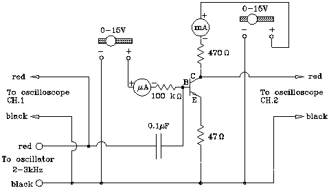
Figure 11:Voltage Amplifier
IE ~ IC = bIB
---------------------Eqn.(4)
From VBE << VCE follows;
VB ~ VE. -------------------Eqn.(5)
Referring to Fig. 11, you see that
VE = RE IE ~ RE bIB
~ VB. ----------------------Eqn.(6)
From this you can calculate the input resistance Rin
of the amplifier. This is an important quantity since it tells
us how much current the input will draw if we apply a voltage
to it.
Rin = VB/IB ~ VE/IB
~ bRE. ------------------Eqn.(7)
A good voltage amplifier should have a large input resistance,
otherwise it would load down the voltage that one wishes to amplify.
It is comforting to see that in our amplifier the current amplification
b, which is of the order of 100, appears
as a multiplicative factor in the expression for this resistance.
You can also calculate IC:
IC = bIB ~ VB/RE.
----------------------Eqn.(8)
The collector voltage VC is obviously given
by
VC = V - IC RC. -------------------Eqn.(9)
But, what you really want to know is not the collector voltage
but the output voltage, which we define as the change of
the collector voltage that results from a given change of the
input voltage. In other words we would like to know DVC
as a function of DVB. Since
V and RC are constants, we can write
DVC = - RC DIc
= - DVB (RC/RE),
--------------------Eqn.(10)
where the minus sign indicates that a positive DIC
gives a negative DVC. We
can now calculate what is called the small signal voltage gain
g of the amplifier
g = DVC/DVB
= - RC/RE ----------------------Eqn.(11)
Note that in this approximation, which holds only for the
case b >> 1, the gain g is independent
of the current gain b and is given
simply by the ratio of two resistors. This is a very desirable
feature:
!The current gain varies from one transistor to the next whereas it is easy to make resistors that have a well defined value.
!The current gain of a transistor varies with the collector current IC, resistors remain constant.
!The current gain of
a transistor varies with temperature. Resistors can be made to
be temperature independent.
We have said above that in many applications the change of a signal is more important than its absolute value. This is especially true for signals that have a time average of zero. Such signals are called a.c. signals, (for a.c. = alternating current). The signals in an audio amplifier are a typical example.