TRANSISTORS AND AMPLIFICATION
INTRODUCTION
With this series of experiments we want to introduce you to some of the basic circuits used in modern electronics. The term electronics encompasses the large variety of devices whose purpose it is to encode, decode, transmit or otherwise process information. Examples are radio and television receivers, calculators, computers, etc., etc.... In addition to resistors and capacitors, with which you may already be familiar, all these devices nowadays contain two kinds of semiconductor elements: diodes and transistors. For a brief description of the subtle quantum mechanical effects on which these elements depend please turn to the Appendix H on Electrical Conduction. Here we will just state that by the addition of small amounts of certain impurities, a process known as doping, it is possible to create ntype materials, in which the charge carriers are mostly negative and ptype materials in which they are mostly positive.
If one dopes the two halves of a single piece of a semiconductor, for example silicon, so that they become, respectively, ptype and ntype material, one creates at the interface between the two halves a pn junction. Such a pn junctions has the remarkable property that it does not obey Ohm's law: If a voltage is applied to the junction as shown in Figure 1a) no current will flow and the junction is said to be backward biased. If the polarity of the applied voltage is reversed, as shown in Figure 1b), the junction becomes forward biased and a current does flow.
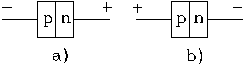
Figure 1: Backward and Forward biased p-n junctions
Devices that consist of a pn junction with leads attached to the nside and the pside, respectively, are known as semiconductor diodes or simply diodes because they have two electrodes, (in Greek the prefix di signifies two or twice). Diodes act as rectifiers i.e. they allow a current to pass through in one direction but not in the other. They are represented by the circuit symbols shown in Figure 2.
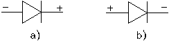
Figure 2: Backward and Forward biased diodes
Now let us look at the circuit shown in Figure 3. It consists of two diodes and no current will flow through it, regardless of the polarity of the applied voltage; either one diode will be backward biased or the other.

Figure 3: Two diodes connected back to back.
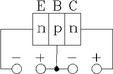
Next we consider the same basic circuit but with a subtle difference: the two np junctions share the same center electrode, i.e. we take a piece of material that is ptype in the middle but ntype on both ends, Figure 4.
Figure 4: Two p-n junctions with a common center electrode
Such a device is called an npn transistor. It is equally possible to start with a piece of ntype material and dope the two ends as ptype, in that case one gets a pnp transistor, either device will work. What does this "circuit" do that the one consisting of two separate diodes does not? Let us assume that we have an npn transistor and that we have applied a voltage so that the np junction on the left is forward biased as shown in Figure 4. Clearly a current will flow into the ntype material and out the ptype center electrode. Now comes the difference: If the ptype center layer is kept very thin many, indeed most, of the charge carriers will simply rush through it and through the second pn junction into the ntype layer on the right side. Once past the obstacle presented by the second junction they are free to move through the ntype material toward the second, even more positive, voltage source. If we reverse the bias on the pn junction on the left, no current can flow into the ptype layer in the center and consequently, no current will flow into the ntype layer on the right side. In other words we have a current amplifier: If we vary the small current from the left electrode, the emitter E, to the center electrode, the base B, then the larger current to the right electrode, the collector C, will vary in proportion. The term "amplifier", although universally used, is a little misleading: the device does not really amplify an electric current, (nothing can do that since electric charge is always conserved in nature), it rather allows us to control a large current with a small one. In circuit diagrams transistors are usually represented by the symbols shown in Figures 5a and 5b. The arrow indicates the direction in which the current flows.
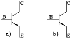
Figure 5: a) pnp transistor and b) npn transistor
You will have noticed that I have glossed over two important points
a) What are the two kinds of charge carriers? The negative carriers
are simply electrons; the positive carriers are holes.
A hole is the absence of an electron in a place were an electron
could be. Why such holes occur in a semiconductor and how they
can act as charge carriers are questions that can only be answered
with the help of quantum mechanics. For an elementary discussions
of the theory of electrical conduction in metals and semiconductors
see Appendix H of this manual or any text on "modern physics"
in the library, e.g. Weidner and Sells (Allyn and Bacon).
b) According to Figure 4 the circuit is symmetrical: If one inverts the polarity of both power supplies one should have a working transistor in which emitter and collector have exchanged their functions. Don't try it! The transistor will indeed work but not nearly as well as with the proper polarity, it may also burn out. The circuit diagram is indeed symmetrical, but the electrodes inside the transistor are not.
To explore transistor circuits experimentally we consider an npn
transistor in the circuit shown in Figure 6. There are three
leads attached to the transistor, this means that we can measure
the three currents in those leads and the three voltages between
the three possible pairs of leads. In an npn transistor, current
flows into the collector and base and out of the emitter. The
collector is most positive, the base intermediate and the emitter
least positive in voltage. We will henceforth use the following
conventions:
VCE = Voltage drop from collector to emitter
VCB = Voltage drop from collector to base
VBE = Voltage drop from base to emitter
IC = Current into the collector
IB = Current into the base
IE = Current out of the emitter.
Since charge can not get lost in the transistor, we know that
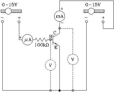
Figure 6: Current amplifier with an npn transistor.
IC + IB = IE. --------------Eqn.(1)
It is also clear that
VCB + VBE = VCE. -------------Eqn.(2)
This means that we need to measure only two voltages and two currents,
as is indicated in the circuit diagram of Fig. 6.
REFERENCES
A suggested reference is Principles of Electronic Instrumentation,
A. James Diefenderfer, pages 143152 and 176190.
APPARATUS
OpAmp Designer Board, Transistor (2N3643), Thornton 6 range
meter (100 mA scale), milliammeter
(025 mA), voltmeter, oscilloscope, 3 resistors (100 kW,
470 W, 47 W),
0.1 mF capacitor, Thornton oscillator.
SOME HELPFUL HINTS
Figure 7 shows the pin connections of the transistor as seen from underneath. Keep in mind that you will be looking at the board and the transistor from above.

Figure 7: Pin connections of the Transistor, bottom view.
The resistance value of a resistor is indicated by four colored bands
using the following color code:
black = 0, brown = 1, red = 2, orange = 3, yellow = 4,
green = 5, blue = 6, purple = 7, grey = 8,
white = 9.
The first band gives the first digit of the resistance value,
the second band the second digit, the third band the number of
zeros following the first two digits, and the fourth band gives
the margin of error allowed to the resistance value: A silver
band indicates an accuracy of "
10 %, and a golden band an accuracy of "
5 %. As a base resistor you should thus use one with a brown band
(1), followed by a black one (0), followed by yellow band (4 zeros)
indicating a resistance of 1 0 0000 or 100 kW.
There should also be a silver band following the yellow, indicating
that the accuracy of the resistance value is
10%.
Use the "OpAmp Designer Board" to put together the circuits that you want to study. Make sure you understand the function of the various controls and the polarity of each element. If you need help please ask your instructor. The relevant components of the designer board and their internal connections are shown in Fig. 8.
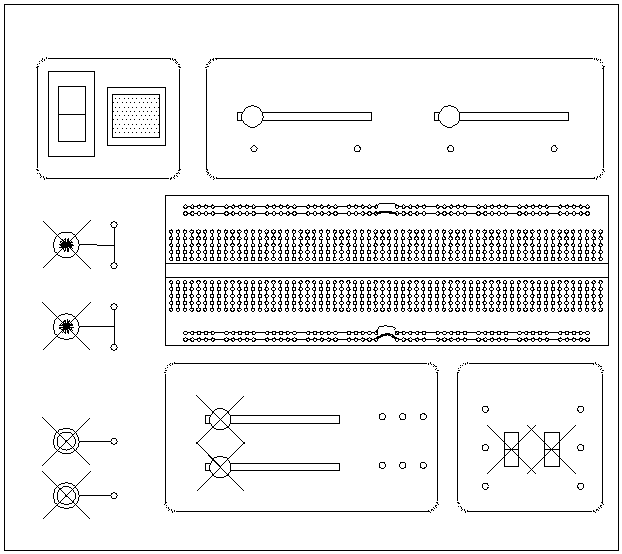
Figure 8: Op-amp designer board. The small circles represent sockets that components can be plugged into. The lines show which of the sockets are interconnected underneath the board. The two upper slide resistors are connected to two independent power supplies whose output voltages, variable between 0 - 15 V, are present at the pin connectors beneath. The components marked with a cross are not used in this experiment. The horizontal rows of sockets should be interconnected in the middle with jumper wires as shown. Use the variable supply on the left to adjust the collector voltage VCE from zero to 10 V.
PLEASE NOTE: The power supplies will put out a maximum voltage of 15 V that can overload the transistor. Don't exceed a collector voltage of 10 V in connection with the circuit shown in Fig. 6.
WHAT TO DO

Figure 9:Designer board with transistor, top view.
MORE HINTS: The milliammeter measures IC, and the voltmeter
can be moved to measure VCE or VBE. The
power supply on the left can be adjusted from zero to 15 V. This
means that the base current, IB, available through
the 100 kW resistor (105 ohms)
in Fig. 6 will vary from zero to 150 microamps, it should be measured
with the Thornton meter. Keep the connecting wires short and
the wiring neat, this will make it easier to find wiring errors,
(don't forget to strip off the insulation at the ends). Lay out
your circuit from the beginning so that you can use it with minor
alterations for all experiments: Identify the emitter lead and
plug it into the top row of one of the columns in the lower half
of the board as shown in Fig. 9 Plug the two remaining leads -
without crossing them - into the bottom row of two different columns
in the top half of the board. Seen from the top the base will
now be on the right and the collector on the left. Use the variable
power supply on the top left of the designer board to supply the
collector voltage, and the one on the right to supply the base
voltage (that way you don't need to cross the wires).
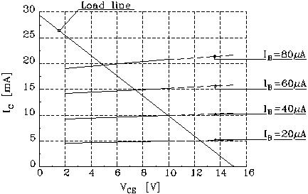
Figure 10:Typical transistor characteristics.
1). Using the circuit shown in Fig. 6, map the characteristics of the transistor by injecting a known current into the base of the transistor. For this first experiment replace the 47 (yellow, purple, black) and the 470 Ohm (yellow, purple, brown) resistors shown in Fig. 9 with short wire bridges. Use the base power supply to set IB to 20 mA. Readjust the slide as necessary to keep IB at that value as you vary VCE with the upper left power supply in steps of 2 volts, while reading IC. Below 2 V the collector current varies very rapidly with the collector voltage. Don't measure in this region, it is outside the normal operating range of the transistor and of no interest. Repeat your measurements for IB = 40, 60, and 80 mA. Do not let the collector current exceed 25 mA or you might damage the transistor. Plot your results to get a set of curves similar to the ones shown in Fig. 10.
Look at your graph. After the steep rise (omitted in your plot)
the collector current levels off. The value of IC in
the flat parts is different for each IB. In fact, if
VCE is held fixed, say at 6 V, IC is nearly
proportional to IB. Check this by calculating the
ratio IC/IB at VCE = 6 V
for each value of IB. This ratio, usually given the
symbol b, is an important parameter
called the base to emitter current gain of the transistor.
b = IC/IB ------------Eqn.(3)
(Taking into account that you measured IC in milliamps
and IB in microamps, b should
be between 50 and 200.) Extract from your plot values of b
at various values of VCE and IC. Does b
change much as a function of either variable? The circuit that
you have built is a (nearly) linear current amplifier: IC
is controlled by IB, is much larger than it and, over
a considerable range, is nearly proportional to IB.
2). Change the leads of the voltmeter to read VBE.
Set the collector voltage VC to 10 V and use the right
slide resistor to vary VBE, (without exceeding IC
= 25 mA) . Note that, even though both base and collector
current vary greatly, VBE remains nearly constant at
about 0.6 V. No matter how much current is drawn, the base
remains at nearly the same potential as the emitter.
Calculate the gain of a voltage amplifier as shown in Fig.
11, using RE = 47 W, and
RC = 470W. This
calculation requires some thought because a changing output
voltage across RC results in a changing collector
voltage VC. In Fig. 11 the voltages are defined with
respect to the negative terminal of the power supply which we
will call common or ground. If we want to refer
to a voltage difference between two arbitrary points we use a
double subscript, i.e. VCE = VC VE.
The currents are defined as before. First note some obvious approximations
that you can make: From IB << IC
follows:
IE ~ IC = bIB
-----------Eqn.(4)
From VBE << VCE follows;
VB ~ VE. ----------------Eqn.(5)
Referring to Fig. 11, you see that
VE = RE IE ~ RE bIB
~ VB. -----------------Eqn.(6)
From this you can calculate the input resistance Rin
of the amplifier. This is an important quantity since it tells
us how much current the input will draw if we apply a voltage
to it.
Rin = VB/IB ~ VE/IB
~ bRE. ---------------Eqn.(7)
A good voltage amplifier should have a large input resistance,
otherwise it would load down the voltage that one wishes to amplify.
It is comforting to see that in our amplifier the current amplification
b, which is of the order of 100, appears
as a multiplicative factor in the expression for this resistance.
You can also calculate IC:
IC = bIB ~ VB/RE.
----------------Eqn.(8)
The collector voltage VC is obviously given
by
VC = V - IC RC. ------------Eqn.(9)
But, what you really want to know is not the collector voltage
but the output voltage, which we define as the change of
the collector voltage that results from a given change of the
input voltage. In other words we would like to know DVC
as a function of DVB. Since
V and RC are constants, we can write
DVC = - RC DIc
= - DVB (RC/RE),
----------------------Eqn.(10)
where the minus sign indicates that a positive DIC
gives a negative DVC. We
can now calculate what is called the small signal voltage gain
g of the amplifier
g = DVC/DVB
= - RC/RE --------------------Eqn.(11)
Note that in this approximation, which holds only for the
case b >> 1, the gain g is independent
of the current gain b and is given
simply by the ratio of two resistors. This is a very desirable
feature:
!The current gain varies from one transistor to the next whereas it is easy to make resistors that have a well defined value.
!The current gain of a transistor varies with the collector current IC, resistors remain constant.
!The current gain of
a transistor varies with temperature. Resistors can be made to
be temperature independent.
We have said above that in many applications the change of a signal is more important than its absolute value. This is especially true for signals that have a time average of zero. Such signals are called a.c. signals, (for a.c. = alternating current). The signals in an audio amplifier are a typical example.
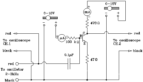
Figure 11: Audio Amplifier
3). Build an a.c. voltage amplifier with a voltage gain of 10. A gain of 10 means that the ratio RC/RE should be equal to 10, as it was in the previous experiment. When no a.c. input voltage is applied, the transistor voltages and currents should be near the center of the operating range that you have determined earlier. Reasonable values would be VC ~ 5 volts, and IC ~ 10 mA, allowing for both a positive and a negative swing of the timevarying output signal. Given a supply voltage of 15 V, a collector voltage of VC = 7.5 V at a current of IC = 10 mA implies a 5 V drop across RC. RC should, therefore, be about 500 W. From RC = 500 W, follows RE = 50 W. The resistors used in the previous experiment, 470 and 47 W, are close enough. Using these values build the circuit of Fig. 11. The 47 W resistor is yellowpurpleblack and the 470 W resistor is yellowpurplebrown. Try to be neat to avoid wiring errors and accidental short circuits between adjacent wires. After you have turned down both power supplies connect them to your circuit. Check the circuit carefully, then turn on the power. Set the collector supply to 15 V, then raise the bias voltage until the bias current is ~ 50 mA. (With the 47 W and the 470 W resistor in series with the transistor it is safe to exceed 10 V on the collector supply.)
When the d.c. voltages and currents have been set you are ready to apply an a.c. signal: Connect one channel of the oscilloscope to the output of the oscillator and set the oscillator output to an amplitude of ~ 0.2 V. Be sure the dc offset control on the oscillator is set to zero. After verifying this value on the scope, connect the oscillator to the amplifier input. Connect the other channel of the oscilloscope to the Output terminal, i.e. to the collector, so that you can simultaneously view both the input and the output waveforms, using the ALT mode of the scope. As you probably know, a d.c. current cannot flow through a capacitor, but an a.c. current can. By using the 0.1 mF capacitor, as shown in Fig. 11, you can introduce an a.c. signal without altering any of the d.c. levels. The amplitude of the output voltage should be 10 times larger than that of the input voltage but cannot be exceed about 6 volts for any input amplitude. Why?
Once you have both the input and the output waveforms on the screen, compare their amplitudes using the calibrated sensitivity setting of the scope. (Be sure the variable sensitivity knobs on the scope inputs are in the fully clockwise CAL position.)
Now take another look at Fig. 10. As IB gets bigger, so does IC. However, a larger value of IC means a smaller value of VCE due to voltage drop across the series resistors, (47 W and 470 W). Indeed, IC cannot possibly get bigger than ICMAX = 15 V/(RC+RE) = 29 ma. Mark this value on your graph. Conversely, a small value of IB implies a small value of IC. A smaller IC in turn means a large value for VCE. The obvious limit is (VCE)max = 15 V, the voltage of the collector power supply. The intermediate values of IC and VEC one finds to lie along a straight line between the extremes. This straight line is the load line, shown in Fig. 10, and you should draw it on your graph.
The supply voltage V must equal the sum of the voltage VCE
across the transistor and the voltage drop across the two resistors
RC and RE.
V = VCE(IC) + IC(RC
+ RB)
We cannot readily solve that equation because we have only the
measured curves for the characteristic VC(IC),
not a mathematical expression. If we write the same equation in
the form
V - IC(RC + RB) = VCE(IC)
we have on the left the mathematical expression for the load line
as a function of the collector current, and on the right the expression
for the measured collector voltage as a function of the collector
current. The equal sign means that both expressions must be true
simultaneously, even if the second one is not known to us in a
mathematical form. We conclude that for any given base current
the collector current must be given by the intersection of the
characteristic for that base current and the load line. In other
words the load line lets us solve graphically the equation
that we could not solve mathematically.
Following are some suggestions for further exploration. Be systematic
and keep careful notes of your observations and measurements.
Take enough time to do a good job and don't feel that you have
to do everything. Be sure to leave the right power supply set
at 15 V.
FOR EXTRA CREDIT
a) Apply an a.c. signal of about 0.05 V amplitude (0.l V peaktopeak)
and vary the bias current IB. Watch the shape
of the output waveform while keeping track of the d.c. part of
VC. This can be done by viewing the output wave on
the oscilloscope with the vertical input coupling turned to d.c.
Note the values of IB, VCE, and the output
amplitude at which the output waveform begins to change.
Can you predict from the measured transistor characteristics where
the distortions will begin?
b) Increase the input amplitude and adjust the bias current until
you have found the largest possible undistorted output amplitude.
Write down this bias current and leave it unchanged. Mark the
corresponding point on your load line and mark the limits of the
swing along the load line when the output is just beginning to
distort. (Note that you are measuring VC while the
graph is in terms of VCE, so you must subtract VE
from VC to plot on the graph.) Can you explain the
distortion in terms of the graph? Can you see why other bias values
might lead to distortions at lower amplitudes?